Trace PCB: A Comprehensive Guide
Par un écrivain mystérieux
Description
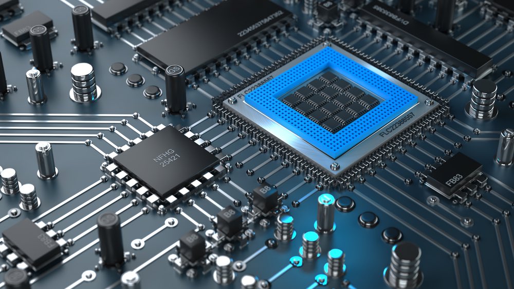
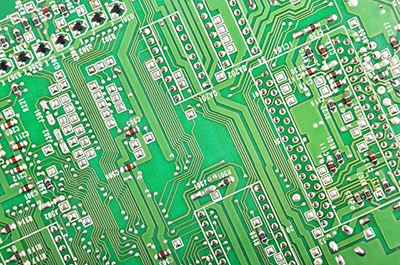
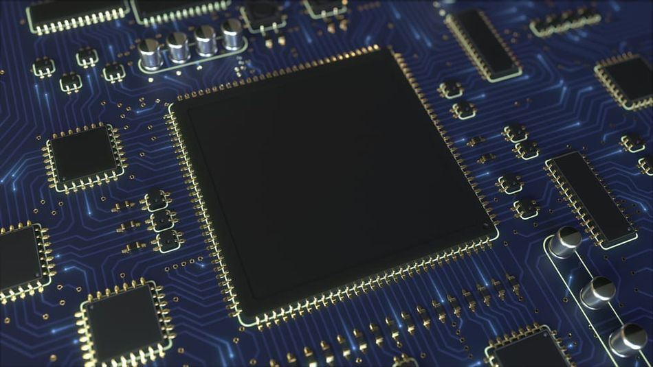
A PCB trace is a highly conductive track that is used to connect components on a printed circuit board. The traces are commonly made of copper and are fabricated during the etching process of a PCB. This article delves into the explanation of PCB trace, its vital components, and its significance to PCB design and fabrication.

How to pick the right Trace Width for PCB design? - PCB Design Tutorial - PCBway
Trace PCB: A Comprehensive Guide
Best Guide To PCB Traces: Width, Thickness And Design Fix Recommendations - Jhdpcb

Unveiling the World of PCB Clone Services: A Comprehensive Guide
Your Guide to All PCB Types [Printed Circuit Boards Explained]

Key Components of a PCB: Layers, Traces, and Pads Explained - Viasion PCB

PCB design - your 10-minute guide to create your PCB - IBE Electronics
Acid Trap PCB Via-Ultimate Guide On All the Things You Need to Know

PCB Pitch: The Ultimate Guide to Crafting an Effective PCB Pitch - MorePCB
Trace PCB: A Comprehensive Guide

PCB silkscreen - a comprehensive guide - PCBA Manufacturers
High-Speed PCB: A Comprehensive Guide
PCB Prices: What You Need to Know [Complete Guide]

The Comprehensive Guide to PCB Reverse Engineering

A complete guide on PCB copper trace - PCBA Manufacturers
depuis
par adulte (le prix varie selon la taille du groupe)